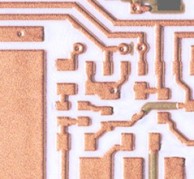
PCTF-Technology
PCTF (Plated Copper on Thick Film) substrates are used in very diffent applications. Plated copper on Thick Film technology allows designers to complement plated copper tracks and thermal vias with thick film multi-layer circuitry, including printed resistors, capacitors and fine line gold. PCTF enables high integration level and miniaturization combining DC power, RF circutry and integrated passive components on the same substrate.
The most typical applications are assembly of surface mount componenets (especilly power SMC), chip-on-board (COB) applications and chip scale packages (chip carriers, flip chip, BGA). Additional applications include SMT multichip modules (MCM), chip carrieres and packages for direct pc board mount as well as hermetic power packages integrating multilayer substrate with plated copper and hermetic vias into a package base (ISP, or Integral Substrate Packages).
Overview metallization
|
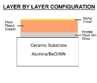
Plated Copper on Thick Film Technology
- With our PCTF technology we reinforce the thick film start layer with electroplated Copper. The most used copper thickness is betwenn 25 µm– 150 µm.
- The finish is depending from the following process like soldering, wire-bonding and glue. NiAu is very often used for soldering and Al-Wire bonding, NiPdAu is an must if you like to do Au-Wire bonding.
- Vias can be hermiticaly close or metallized only
- Multilayer thick film substrates can get an additional layer of Cu and NiAu or NiPdAu.
|
 |
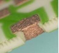
Wraparound / Castellations for SMT Attach
- Castellations enable large chip carrier (>10x10mm) for direct PCB attachment
- High conductance
- Low inductance
- High relaible connections
|

|
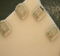
Stand Off / Bump for SMT Attach
- Solder bumps - SMT / Direct PCB attachment
- Electro plating thickness from 3 µm to 50 µm
- Beside Copper we can do (Gold / Tin) Au/Sn 78/28 to 80/20 also
- AuSn platting reduce the costs for soldering, no usage of preformce
- This mean soldering of Laser-Submounts, Combo Lids, LED and Packages is cheaper
|
 |
|
Plugged Vias (PowerPlug
- Powerplug vias are fully hermetic and withstand gross and fine leak test
- Thermische Vias haben eine Leitfähigkeit von 200 W/mk.
- Plugged via holes provide excellent electrical interconnections (signal and ground)
- Combined with PFTF serve as thermal heat pipes while ensuring low thermal pesistance from top to bottom
|
 |
|
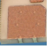
Thick Copper Tracks and plated copper pads with plugged vias
- Plated copper tracks and pads with plugged vias allows a higher power and circuit density
- Provide high current carring capacity (to 50 Amps)
- Low conductor resistance, 0.6 to 0.07 mohm/square
- Heat sprading effect help to increase the live time of semiconductors
- CTE mismatch is reduced. CTE value from AL2O3 is 6,4 – 7,0 ppm/°C, BeO 7,0 ppm/°C and from AIN 4,6 ppm/°C.
|
 |


