Thick Film Circuits and Hybrid Circuits
Our service, development, production and delivery of thick film and hybrid circuits
Thick film technology is the basic for the production of electronic devices such as hybrid intergrated circuits, sensors, surface mount devices.
Thick film circuits are widely used in the automotive industry, both in sensors, e.g. mixture of fuel/air, pressure sensors, engine and gearbox controls, sensor for releasing airbags, ignitors to airbags; common is that high reliability is required, often extended temperature range also along massive thermocycling of circuits without failure.
The manufacture of such devices is an additive process involving deposition of several successive layers of conductor, resistors and dielectric layers onto an electrically insulating substrate using a screen-printing and fireing process.
A typical thick film process would consist of the following stages:
- Prepare Al2O3, AIN or stainless stell substrateseenless
- Prepare the ink and do screen printing
- Drying/Curing and firing the paste
- Laser trimming of resistors
- Mounting of SMT components like resitors, capacitors and semiconductors
- Separation in single elements
- Intergate in an device
Advantages of Thick Film Circuits and Hybrid Circuits:
- Very compact, stabil and robust
- Ceramic substrates an very good low-loss isolator. The loss power disappear over the total substrate
- Printed and laser trimmed resistors are very accurate they are better as 0,1%
- Usable in high temeratur application and in very rough environments
- Usable in an vacuum and in areas with high vibrations
Tick Film Hybrids easy to produce with a short delivery time and for low costs
We are looking forward to receive your inquiry.
Our support includes development, implementation, production and test.
Download brochure "Thick Film and Hybrid Circuits"
|
Hybrid Assembly
|
 |
|
Assembly COB Process
|
 |
|
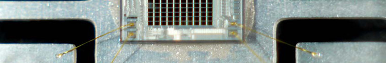
Assembly, Wire Bonding
|
 |
|
Wire Bonding
|
 |
|
Hybrid, coated and un coaded
|
 |